
Get a Quote

PCB / PRODUCT KNOWLEDGE

Multilayer PCB

Multiple copper layers and an agreed stack-up for interconnected designs.

← All PCB categories
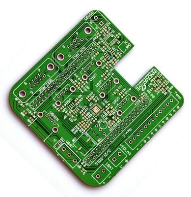
Multilayer PCB product photograph
Multilayer PCB product photograph.

UNDERSTAND THE CONSTRUCTION

Understanding Multilayer PCB

A multilayer PCB incorporates internal copper layers between its outer surfaces. Signal layers and reference planes can be arranged to support a more connected design. The layer count alone does not define electrical performance: the complete stack-up, materials and routing constraints matter.

Product scope
The store has multilayer board listings. Rigid PCB is treated as a broader, overlapping shop group rather than a duplicate independent-site category. The construction explanation is general guidance. Final materials, manufacturing limits and availability require engineering confirmation.

Discuss this board type

PRODUCT LISTINGS & PHOTOGRAPHY

Explore the actual product brief.

The store has multilayer board listings. Rigid PCB is treated as a broader, overlapping shop group rather than a duplicate independent-site category.

OBEST / STORE PRODUCT

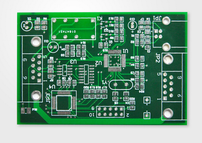
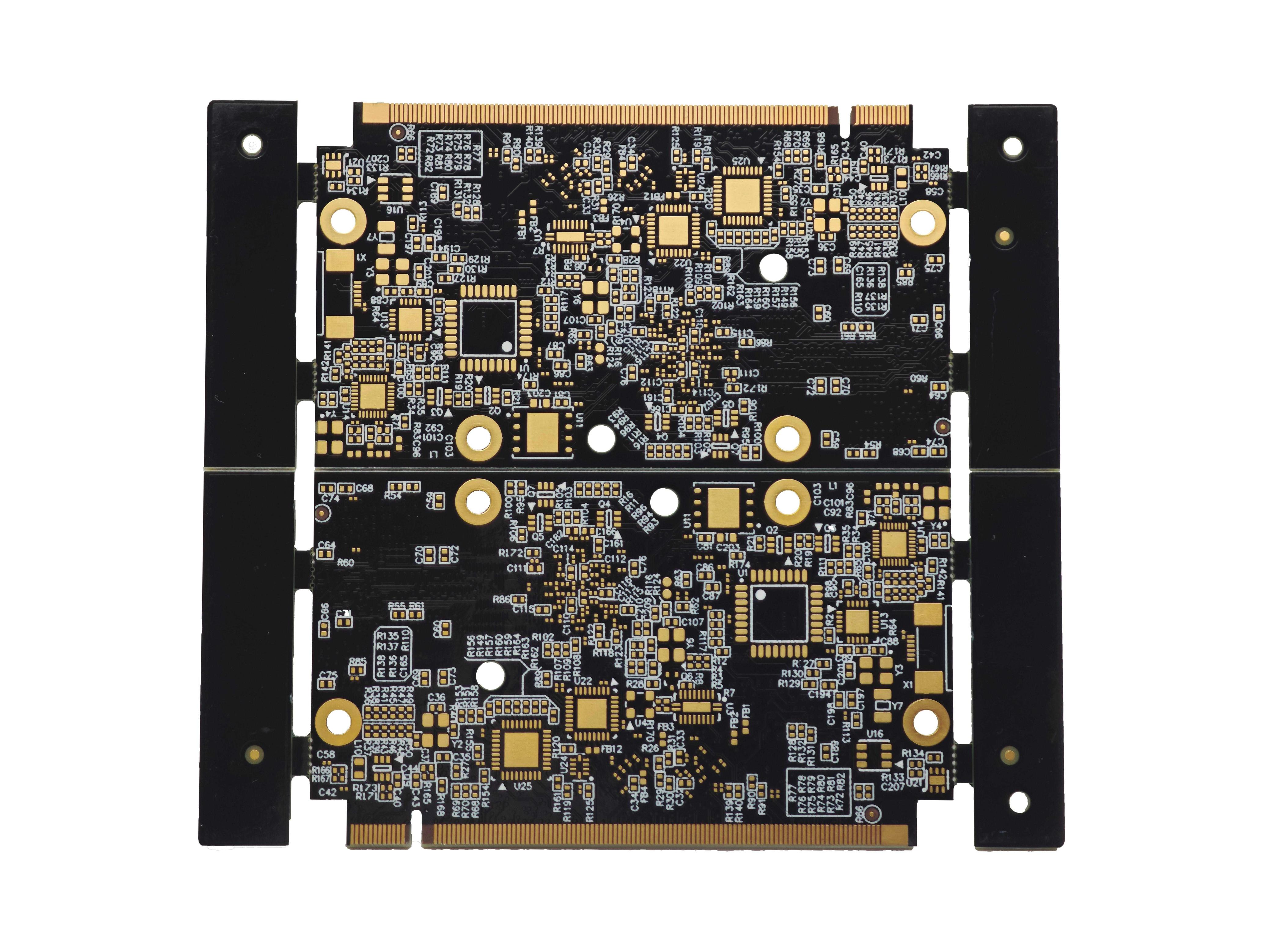
Custom multilayer PCB & assembly

Listing reference 1601766802876

View source listing ↗

A custom multilayer board and assembly listing. The product page identifies the model as Multilayer PCB and offers configurable construction for review.

Model
Multilayer PCB
Layer range stated for this listing
2–32 layers
Board thickness stated for this listing
0.2–6 mm
Finish options stated for this listing
HASL / OSP / Ag / ENIG / ENEPIG / immersion silver / tin

Select the layer count, material, stack-up and surface finish for the specific build. These details belong to this listing only. Confirm the final construction, acceptance criteria and availability for your project.
STRUCTURE & DESIGN CONSIDERATIONS

What makes it different.

Construction choices should follow the design intent and an agreed engineering review.

01

An agreed stack-up

Document the order of signal and plane layers, dielectric construction and target finished thickness before release.

02

Signal reference planning

Identify signals that require controlled impedance and their reference layers. Any target needs a defined tolerance and an approved construction.

03

Via and plane coordination

Share via structures, plane clearances and any back-drilling requirements for a feasibility review; these options are not confirmed here.

TYPICAL APPLICATIONS

Where this approach may fit.

Connected control systems

Processors, memory and multiple interfaces can create routing and power-distribution needs that favor internal layers.

Communication hardware

Signal integrity and reference-plane planning may influence the stack-up; the design must be reviewed for its actual interfaces.

Examples describe general design uses. Company sector experience, application suitability and qualifications pending confirmation / 待确认.

PREPARE YOUR INQUIRY

Bring the right information.

Read the RFQ preparation guide ↗
  • Layer-mapped Gerbers, drill files and a controlled fabrication drawing.
  • Proposed stack-up, material requirements and finished copper definition.
  • Impedance targets with the relevant layer, geometry, reference plane and tolerance.
  • Via requirements, critical dimensions and quantities for each build stage.

COMPANY VERIFICATION

Capabilities to confirm.

These rows identify topics for discussion. They are not published manufacturing limits.

Multilayer PCB requirements — request inputs and company verification status
ParameterWhat to specify for reviewCompany capability
Product availabilityBoard type, intended use and project revisionPending confirmation / 待确认
Layer countLayer order, reference planes and proposed stack-upPending confirmation / 待确认
Board dimensionsFinished outline, cut-outs and critical tolerancesPending confirmation / 待确认
MaterialsMaterial designation or performance requirements; alternatives need approvalPending confirmation / 待确认
Board thicknessFinished thickness and tolerancePending confirmation / 待确认
Copper weightInner / outer copper and finished or starting copper definitionPending confirmation / 待确认
Trace / spaceSmallest features and any locally critical geometryPending confirmation / 待确认
Drill sizeFinished hole sizes, plated status and drill spansPending confirmation / 待确认
Surface finishesRequested finish, storage or assembly constraintsPending confirmation / 待确认
Solder mask colorsRequested color and any appearance requirementsPending confirmation / 待确认

CONTINUE EXPLORING

Related board categories.

Planning assembly too? ↗

LET’S BUILD WHAT’S NEXT

Your next board starts
with a conversation.

Bring your requirements. Identify what needs engineering review.

Get a Quote