
PCB CAPABILITIES
PCB Manufacturing Capabilities
Company-provided PCB process parameters, from material selection and lamination to drilling, imaging and profiling. Review the full construction and process combination for your design.
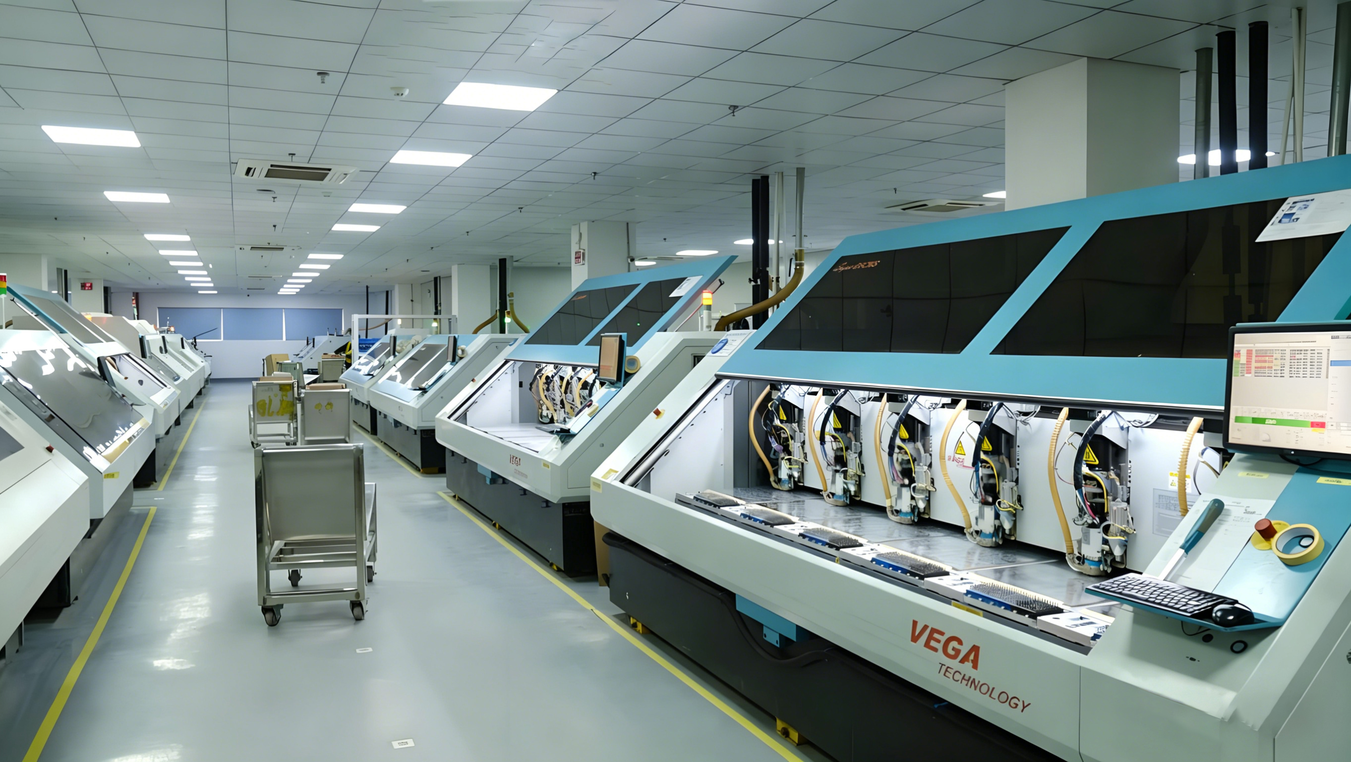
OBEST / PROCESS PHOTOGRAPHY
PCB drilling equipment.
OBEST / COMPANY-PROVIDED DATA
PCB Manufacturing Capabilities
Selectable text · On smaller screens, scroll horizontally to view every column.
| Process | Parameter | Capability |
|---|---|---|
| Materials | Materials | Shengyi, ITEQ, SOLA, Rogers, Panasonic, Teraoka |
| Cutting | Maximum panel size | 500 × 600 mm |
| Lamination | Lamination layer count | 4–62 layers |
| Inner Layer | Minimum line width/spacing | 2/2 mil |
| Base copper thickness | 1/3–6 oz | |
| Alignment | ±0.05 mm | |
| Graphic to board edge | 0.5 mm | |
| Drilling | Minimum drill bit size | 3.8 mil |
| Maximum drill bit size | 152.4 mil | |
| Minimum hole diameter | 2.54 mil | |
| Metallized-hole dimensional tolerance | ±3 mil | |
| Non-metallized-hole dimensional tolerance | ±2 mil | |
| Outer Layer | Minimum line width/spacing | 0.076/0.076 mm |
| Base copper thickness | 1/3–12 oz | |
| Interlayer alignment | ±0.05 mm | |
| Impedance control tolerance | ±10% | |
| Line-to-line spacing | 0.08 mm | |
| Line-to-pad distance | 0.1 mm | |
| Pad-to-pad distance | 0.1 mm | |
| Solder Mask | Opening to line edge | 0.1 mm |
| Minimum solder mask dam | 0.1 mm | |
| Alignment | ±0.05 mm | |
| Silkscreen | Minimum character width | 0.13 mm |
| Minimum character height | 0.8 mm | |
| Surface Treatment | Finish thickness specifications | Pending clarification |
| Routing & Profiling | Minimum routing bit size | 0.8 mm |
| Maximum routing bit size | 1.6 mm | |
| Routing tolerance | 0.1 mm | |
| Punching tolerance | 0.05 mm | |
| V-cut angle tolerance | +5° | |
| V-cut remaining thickness tolerance | ±0.05 mm | |
| Minimum V-cut size | 30 × 30 mm |
Capabilities depend on the material, stack-up and process combination. Final feasibility is confirmed after engineering review.
The 4–62 layer range refers to lamination only; it does not replace the single- and double-sided product categories. Surface-treatment thickness data is awaiting clarification. PCB board thickness and solder mask colors are not specified in this data.
Individual limits must be reviewed in combination. These figures do not imply that every maximum or minimum can be achieved simultaneously. Other assembly processes, test coverage and delivery arrangements require project-specific confirmation.
Prepare requirements for reviewLET’S BUILD WHAT’S NEXT
Your next board starts
with a conversation.
Bring your requirements. Identify what needs engineering review.