
Get a Quote

PCB / PRODUCT KNOWLEDGE

HDI PCB

High-density interconnect board projects; build-up and via structure require review.

← All PCB categories
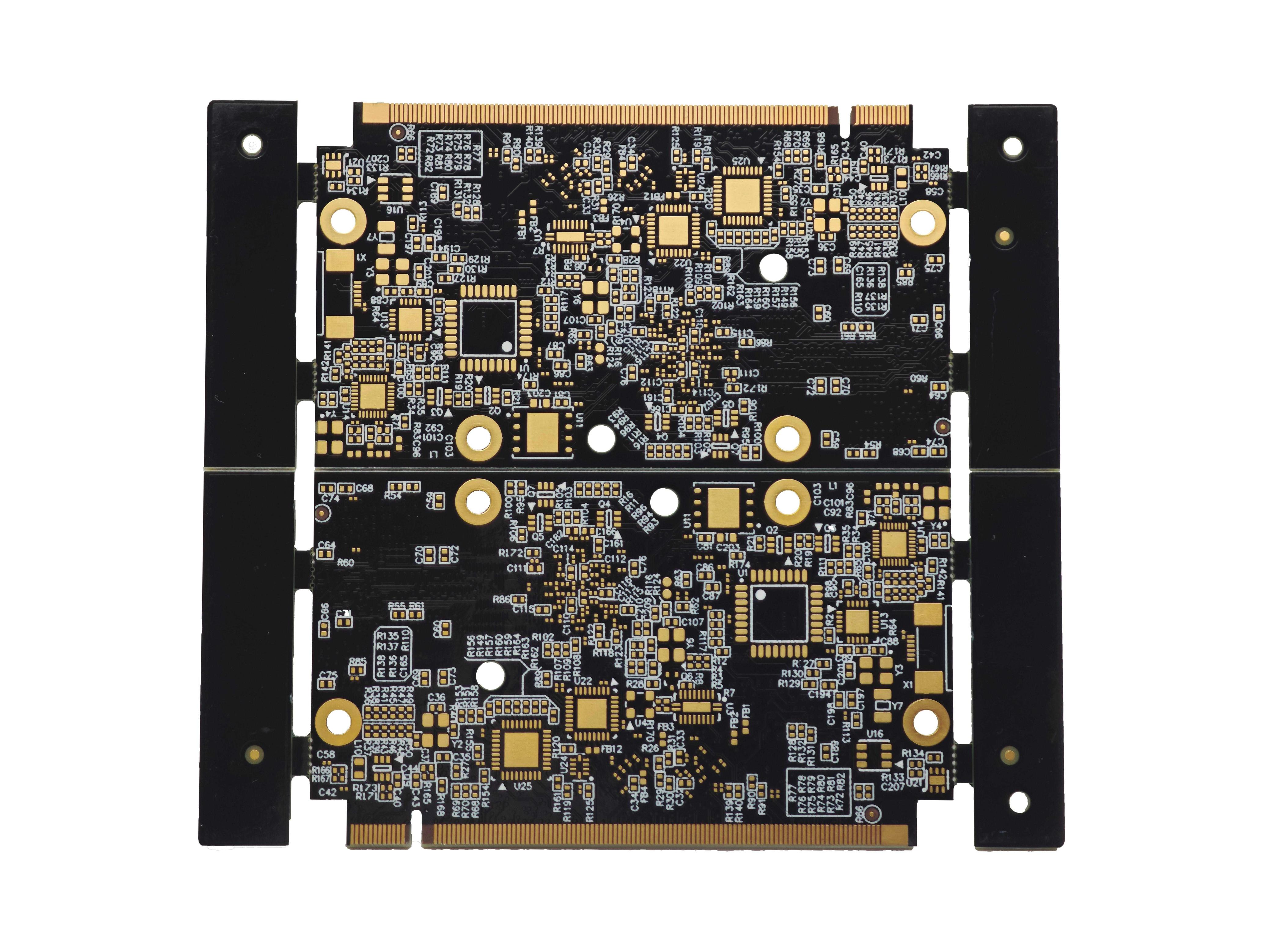
HDI PCB product photograph
HDI PCB product photograph.

UNDERSTAND THE CONSTRUCTION

Understanding HDI PCB

High-density interconnect designs use interconnection structures intended for compact routing, often around fine-pitch devices. Microvias and sequential build-up may be involved. HDI is a construction approach rather than a universal specification, so the intended layer and via structure must be reviewed explicitly.

Product scope
The HDI store category and an HDI-titled product were reviewed. Microvia structure, build-up and actual HDI limits still need project confirmation. The construction explanation is general guidance. Final materials, manufacturing limits and availability require engineering confirmation.

Discuss this board type

PRODUCT LISTINGS & PHOTOGRAPHY

Explore the actual product brief.

The HDI store category and an HDI-titled product were reviewed. Microvia structure, build-up and actual HDI limits still need project confirmation.

OBEST / STORE PRODUCT

Custom HDI PCB project listing

Listing reference 1601777472982

View source listing ↗

An OBEST product titled HDI PCB, listed in the store’s Multilayer PCB group. The page describes a customized board and assembly project rather than a fixed, fully defined HDI build-up.

Material field
FR-4
Board thickness field
1.4 mm
Copper thickness field
1 oz
Application field
Electronics Device

Provide the proposed HDI build-up and via structure for engineering review. These details belong to this listing only. Confirm the final construction, acceptance criteria and availability for your project.
STRUCTURE & DESIGN CONSIDERATIONS

What makes it different.

Construction choices should follow the design intent and an agreed engineering review.

01

Device-driven escape routing

Package pitch, pad layout and fan-out constraints influence the interconnect strategy. Supply the relevant component land-pattern information.

02

Build-up definition

Describe the proposed layer sequence and any blind, buried, stacked or staggered vias. Do not assume these constructions are interchangeable.

03

Via-in-pad requirements

State whether filling, capping or other pad treatments are needed. Availability and inspection criteria need confirmation.

TYPICAL APPLICATIONS

Where this approach may fit.

Compact processing modules

Dense processors and memory can motivate a smaller interconnect structure when conventional routing is insufficient.

Space-constrained assemblies

Portable and miniature electronics may use HDI after electrical, assembly and reliability review.

Examples describe general design uses. Company sector experience, application suitability and qualifications pending confirmation / 待确认.

PREPARE YOUR INQUIRY

Bring the right information.

Read the RFQ preparation guide ↗
  • Full layer data, drill spans and a proposed build-up drawing.
  • Fine-pitch package information and the smallest design features requiring review.
  • Microvia topology, via-in-pad treatment and intended qualification criteria.
  • Controlled impedance requirements, material selection and revision-controlled drawings.

COMPANY VERIFICATION

Capabilities to confirm.

These rows identify topics for discussion. They are not published manufacturing limits.

HDI PCB requirements — request inputs and company verification status
ParameterWhat to specify for reviewCompany capability
Product availabilityBoard type, intended use and project revisionPending confirmation / 待确认
Layer countLayer order, reference planes and proposed stack-upPending confirmation / 待确认
Board dimensionsFinished outline, cut-outs and critical tolerancesPending confirmation / 待确认
MaterialsMaterial designation or performance requirements; alternatives need approvalPending confirmation / 待确认
Board thicknessFinished thickness and tolerancePending confirmation / 待确认
Copper weightInner / outer copper and finished or starting copper definitionPending confirmation / 待确认
Trace / spaceSmallest features and any locally critical geometryPending confirmation / 待确认
Drill sizeFinished hole sizes, plated status and drill spansPending confirmation / 待确认
Surface finishesRequested finish, storage or assembly constraintsPending confirmation / 待确认
Solder mask colorsRequested color and any appearance requirementsPending confirmation / 待确认

CONTINUE EXPLORING

Related board categories.

Planning assembly too? ↗

LET’S BUILD WHAT’S NEXT

Your next board starts
with a conversation.

Bring your requirements. Identify what needs engineering review.

Get a Quote