
Get a Quote

PCB / PRODUCT KNOWLEDGE

Double-side PCB

Copper circuitry on both sides of the board, connected as the design requires.

← All PCB categories
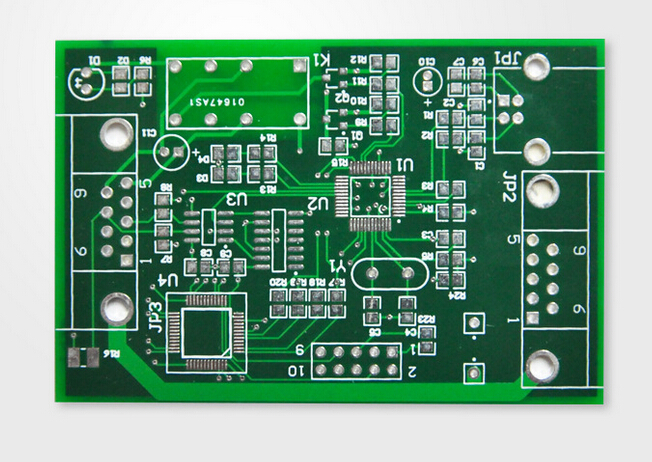
Double-side PCB product photograph
Double-side PCB product photograph.

UNDERSTAND THE CONSTRUCTION

Understanding Double-side PCB

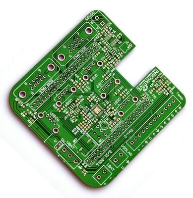
A double-sided PCB carries copper circuitry on the top and bottom of an insulating core. Connections between the two sides are commonly made through plated holes. This structure can give a design more routing freedom than a single-sided board while keeping the layer arrangement straightforward.

Product scope
Double-sided board products are listed in the OBEST store. The featured image is a multi-design product selection, not one fixed board specification. The construction explanation is general guidance. Final materials, manufacturing limits and availability require engineering confirmation.

Discuss this board type

PRODUCT LISTINGS & PHOTOGRAPHY

Explore the actual product brief.

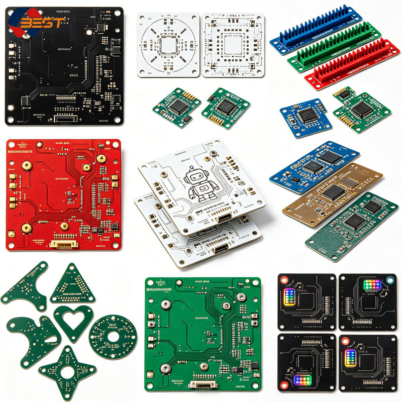
Double-sided board products are listed in the OBEST store. The featured image is a multi-design product selection, not one fixed board specification.

OBEST / STORE PRODUCT

Custom FR-4 double-sided PCB

Listing reference 1601946861869
View source listing ↗
OBEST PCB and PCBA product selection from listing 1601946861869; several designs pictured

An OBEST listing for customized double-sided and multilayer board design. Its product image shows a selection of bare boards and assembled electronic designs; it does not represent one fixed configuration.

Material in listing title
FR-4
Thickness in listing title
1.6 mm
Application field
EV / BMS / Solar Inverter
Service field
Turnkey PCBA and BOM component sourcing

Specify the finished thickness, layer count and material in the fabrication drawing. These details belong to this listing only. Confirm the final construction, acceptance criteria and availability for your project.
STRUCTURE & DESIGN CONSIDERATIONS

What makes it different.

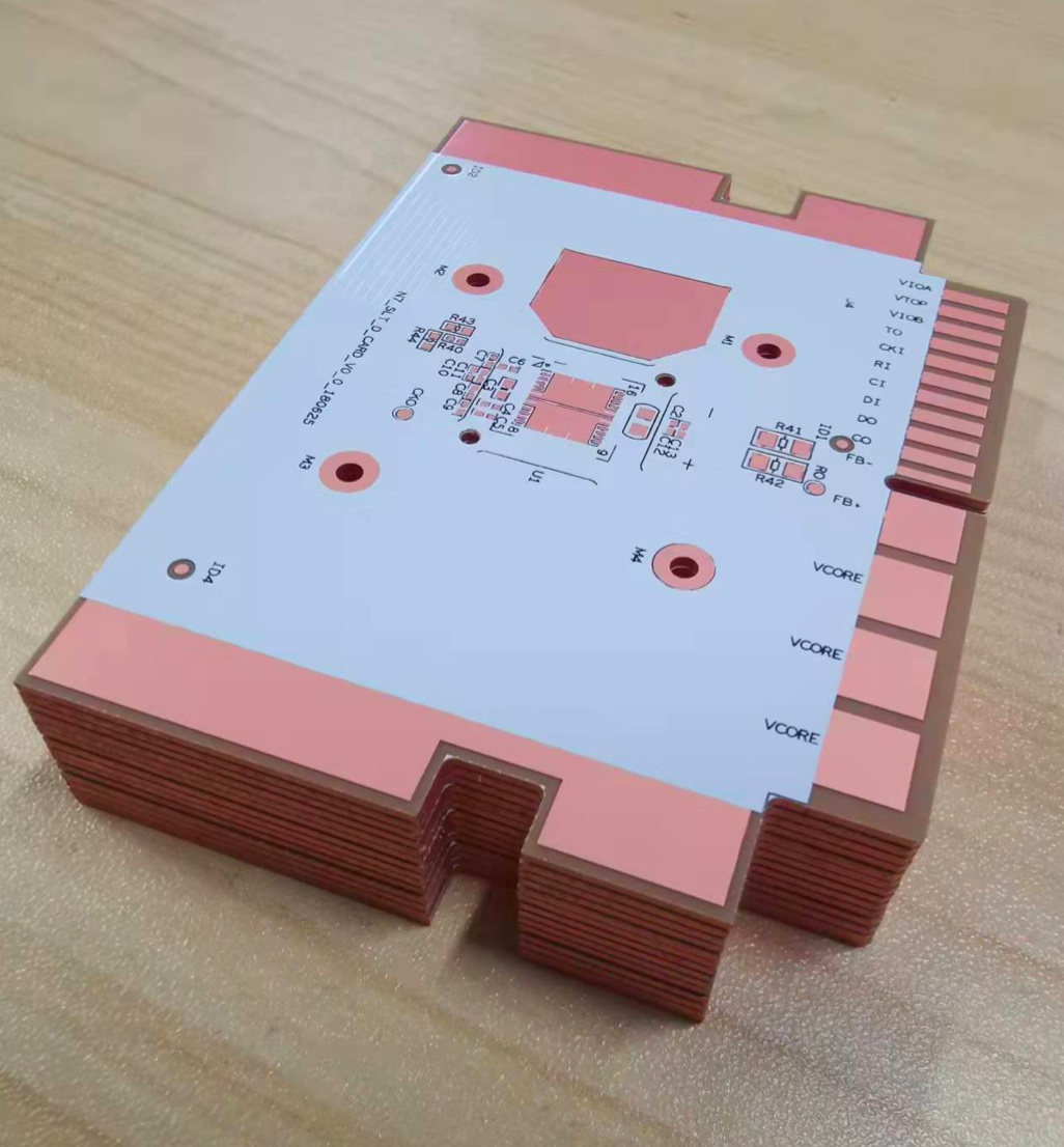
Construction choices should follow the design intent and an agreed engineering review.

01

Two copper layers

Top and bottom routing share one core. Identify which signals, components and copper areas belong on each side.

02

Interlayer connections

Separate plated connections from non-plated mechanical holes in the fabrication data. Hole dimensions and tolerances need agreement.

03

Assembly access

Component placement, connector clearance and test access should be reviewed alongside the board outline.

TYPICAL APPLICATIONS

Where this approach may fit.

Control interfaces

Switches, indicators and connectors may use a two-sided layout when routing and electrical requirements permit.

Sensor and interface boards

Simple sensing and signal interface circuits can be considered after reviewing noise, current and mechanical requirements.

Examples describe general design uses. Company sector experience, application suitability and qualifications pending confirmation / 待确认.

PREPARE YOUR INQUIRY

Bring the right information.

Read the RFQ preparation guide ↗
  • Gerber ZIP and drill data for the same revision, including the board outline.
  • Requested core material, finished board thickness, copper weight and finish.
  • Plated / non-plated hole identification and critical mechanical tolerances.
  • Order quantity, panel preference and any electrical test requirements.

COMPANY VERIFICATION

Capabilities to confirm.

These rows identify topics for discussion. They are not published manufacturing limits.

Double-side PCB requirements — request inputs and company verification status
ParameterWhat to specify for reviewCompany capability
Product availabilityBoard type, intended use and project revisionPending confirmation / 待确认
Layer countLayer order, reference planes and proposed stack-upPending confirmation / 待确认
Board dimensionsFinished outline, cut-outs and critical tolerancesPending confirmation / 待确认
MaterialsMaterial designation or performance requirements; alternatives need approvalPending confirmation / 待确认
Board thicknessFinished thickness and tolerancePending confirmation / 待确认
Copper weightInner / outer copper and finished or starting copper definitionPending confirmation / 待确认
Trace / spaceSmallest features and any locally critical geometryPending confirmation / 待确认
Drill sizeFinished hole sizes, plated status and drill spansPending confirmation / 待确认
Surface finishesRequested finish, storage or assembly constraintsPending confirmation / 待确认
Solder mask colorsRequested color and any appearance requirementsPending confirmation / 待确认

CONTINUE EXPLORING

Related board categories.

Planning assembly too? ↗

LET’S BUILD WHAT’S NEXT

Your next board starts
with a conversation.

Bring your requirements. Identify what needs engineering review.

Get a Quote